


A outstanding proof-of-concept undertaking has efficiently manufactured nanoscale diodes and transistors utilizing a quick, low cost new manufacturing approach by which liquid metallic is directed to self-assemble into exact 3D buildings.
In a peer-reviewed research on account of be launched within the journal Supplies Horizons, a North Carolina State College group outlined and demonstrated the brand new methodology utilizing an alloy of indium, bismuth and tin, often known as Area’s metallic.
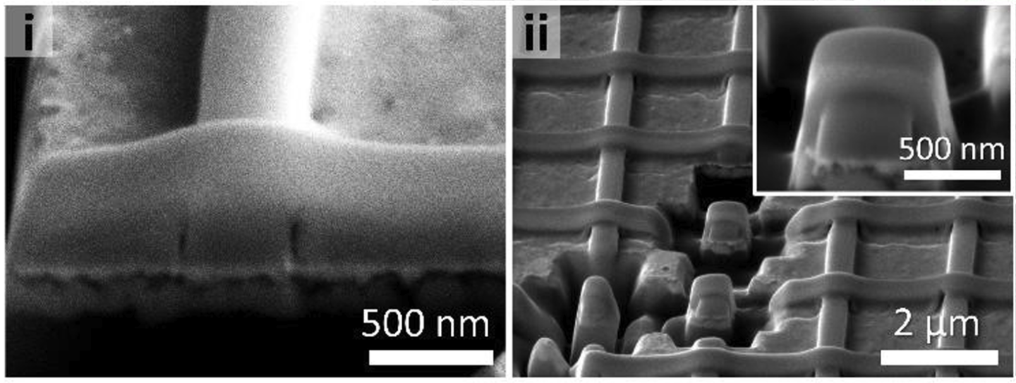
The liquid metallic was positioned beside a mould, which the researchers say might be made in any dimension or form. Because it’s uncovered to oxygen, a skinny oxide layer varieties on the floor of the metallic. Then, a liquid is poured onto it, containing negatively-charged ligand molecules designed to drag particular person metallic atoms off that oxide layer as positively-charged ions, and bind with them.
These metallic ions held within the ligands change into somewhat like magnetic constructing blocks, attracted to 1 one other, and because the ligand answer begins to movement by channels within the mould, pushed by capillary motion, it pulls these constructing blocks by with it. The mould primarily will get the blocks to line up into orderly buildings, like wires, and stick to one another in place.
Julia Chang/NC State College
“With out the mould, these buildings can kind considerably chaotic patterns,” says Martin Thuo, corresponding writer and professor of supplies science and engineering at North Carolina State College. “However as a result of the answer is constrained by the mould, the buildings kind in predictable, symmetrical arrays.”
As soon as every part is in place, the liquid a part of the ligand answer begins to evaporate, which has the impact of compacting the ligands and metallic ions even nearer collectively of their channels. Then the mould is taken away, and the ultimate form is slowly heated to round 600 °C (1,112 °F) and stored there for an hour.
This heating course of provides sufficient vitality to interrupt the chemical bonds holding the ligand molecules collectively, so carbon and oxygen atoms are launched.
The oxygen instantly bonds to the metallic ions, forming semiconductor metallic oxides that fuse along with each other in a sintering course of to kind wires. The carbon atoms, in the meantime, manage themselves into graphene, which wraps neatly across the wires to enhance their electrical conductivity, defending them from moisture or additional oxidation.
Julia Chang/NC State College
The researchers demonstrated they’ll additionally use these graphene layers to tweak {the electrical} and optoelectric properties of the ensuing wires. “The graphene sheets can be utilized to tune the bandgap of the semiconductors, making the semiconductor roughly responsive, relying on the standard of the graphene,” says Julia Chang, first writer of the paper and a postdoctoral researcher at NC State.
Regardless that the heating course of causes “extreme quantity shrinkage,” the ensuing wires stay steady and do not break.
“Briefly, we’ve proven that we are able to self-assemble extremely structured, extremely tunable digital supplies to be used in useful digital gadgets,” says Thuo. “This work demonstrated the creation of transistors and diodes. The following step is to make use of this system to make extra complicated gadgets, comparable to three-dimensional chips.”
“The character of the D-Met (directed metallic ligand) approach,” he continues, “means you may make these supplies on a big scale – you’re solely restricted by the dimensions of the mould you employ.”
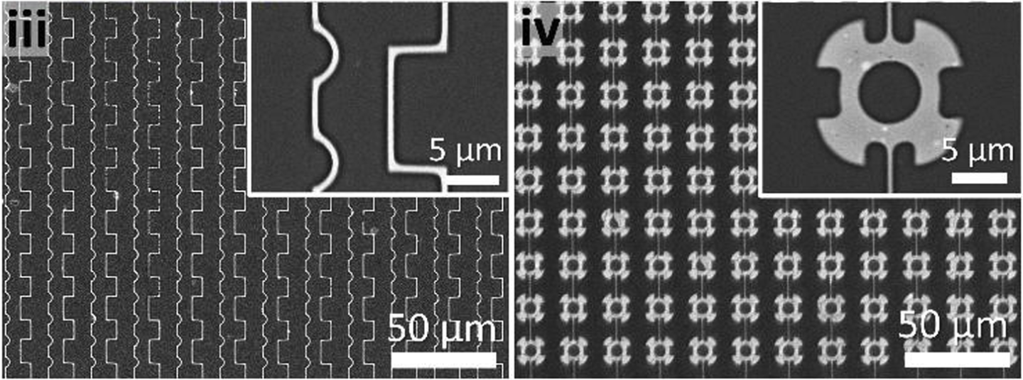
Julia Chang/NC State College
The group says the approach presents a sooner, cheaper, extra dependable means of creating pc chips. “Present chip manufacturing strategies contain many steps and depend on extraordinarily complicated applied sciences, making the method pricey and time consuming,” says Thuo. “Our self-assembling strategy is considerably sooner and cheaper. We’ve additionally demonstrated that we are able to use the method to tune the bandgap for semiconductor supplies and to make the supplies attentive to gentle – which means this system can be utilized to create optoelectronic gadgets.
“What’s extra, present manufacturing strategies have low yield, which means they produce a comparatively giant variety of defective chips that may’t be used. Our strategy is excessive yield – which means you get extra constant manufacturing of arrays and fewer waste.”
It is a fairly outstanding piece of labor – however within the electronics sport, dimension is vital. Take a fast scan by the outstanding video under to get a way for just how tiny the ‘wires’ in a modern CPU chip need to be.
How are Microchips Made? 
 CPU Manufacturing Course of Steps
The state-of-the-art manufacturing strategies utilized by producers like Taiwan’s TSMC can produce options with minimal dimensions as small as 3 nm – or in regards to the width of 15 particular person silicon atoms. It is completely staggering that this mass-manufacturing is going on so near the individual-atom scale, however the smaller it will get, the sooner and extra environment friendly the ensuing chip can change into.
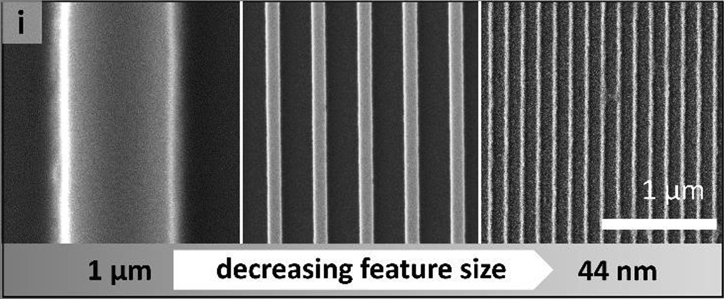
How does this ‘self-assembling’ know-how stack up in opposition to that? Effectively, within the printed research, the researchers managed to efficiently fabricate wires from about 1,000 nm all the best way all the way down to 44 nm.
Julia Chang/NC State College
That is fairly unbelievable; it is a correct nanoscale-capable manufacturing approach that is sooner, cheaper and extra dependable than at present’s finest strategies, even when it will possibly’t but compete on atomic-scale ultimate decision. It is unclear whether or not the D-Met approach might be tailored to work at even smaller scales – however the analysis group believes it is properly and really able to scaling up when it comes to mass manufacturing.
The paper is open entry, post-peer assessment and pre-publication within the journal Materials Horizons.
Supply: North Carolina State University